- Overview
- Specifications
- Downloads
- Featured Products
- Request a Quote
- Product Support
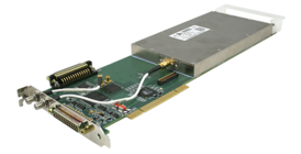
The RMDS-500S combines the functions of RF receiver, demodulator, bit synchronizer, data decommutator, and simulator into a single full-size PCI bus card. The card can be installed in a Desk Top PC for preflight or lab test.
The RF Receiver has L, S or C band coverage (select at build) with a frequency step size of 250 kHz. The Receiver performs a frequency translation from the RF frequency to a 70 MHz IF with Tier 2 phase noise performance. This IF signal is passed through one of five bandpass filters (1.5, 5.0., 14, 20, and 40 MHz). The filtered 70 MHz is output from the Receiver and looped back into the 70 MHz IF Demodulator via an external MCX/MCX coax cable. AGC and AM outputs are also available for tracking applications.
The Demodulator input accepts the 70 MHz output from the Receiver or an external 70 MHz signal (-45 to 0 dBm) and can demodulate SOQPSK, PCM/FM, QPSK, OQPSK, and BPSK. Digital baseband filtering is automatically adjusted based on modulation type and bit rate. The demodulated 70MHz IF signal is input to the Bit Synchronizer.
The Bit Sync has four inputs: the Demod output, TTL, RS422, and Analog. Data rates up to 40 Mbps (SOQPSK, QPSK, and OQPSK), 20Mbps (PCM/FM and BPSK), and 30 Mbps (TTL, RS422, and Analog) can be processed. The Bit Sync performs clock reconstruction and
data recovery. NRZ-(L/M/S) and BiØ-(L/M/S) data can be decoded and/or encoded. Data and clock outputs are provided via RS422 and TTL drivers.
The Bit Sync output is also internally connected to the on-card Data Decommutator. The Data Decommutator provides full IRIG Frame Synchronization and data Decommutation. The Decom accepts PCM data at rates up to 40 Mbps from either an external source or the on-card Bit Sync. The Decom external data and clock inputs are programmable for RS422 (120 ohms) or TTL (50 ohms).
Decommutated data words and frame time tags are made available via the PCI bus for analysis, archival, and monitoring. A Parallel Output Port provides the customer with the Frame Data and control signals. The customer can Cherry Pick any or all desired words from the Frame.
A DB25 connector is used for each Parallel Output Port (top of the card) and the I/O port (rear of the card on rear I/O plate). The rear I/O plate is also equipped with two SMA connectors, for the RF Receiver and Analog Bit Sync input.
Key Features
- PC-based bus full-size card with RF Receiver, Demodulator, Bit Synchronizer, Data Decommutator, Simulator, and IRIG Time Code Reader
- 32 Bit/66 Mhz PCI bridge
- Transfers data in scatter-gather mode
- RF Receiver
- L-band, S-band, and C-band coverage (select at build)
- Selective tuning with 250 kHz tuning steps
- 5 IF bandwidths; 1.5 to 40 MHz
- AGC and AM outputs
- 70 MHz IF output
- 70 MHz Demodulator
- Input: RF receiver or external 70MHz
- Processes: SOQPSK, PCM/FM, OQPSK, QPSK, and BPSK
- Bit Synchronizer
- Inputs: Demod, TTL, RS-422, and analog
- Data rates to 40 Mbps
- I/O codes: NRZ-(L, M, S), BIØ-(L, M, S), RNRZ-L
- Bit error rate tester for PRN (15)
- IRIG-B time code reader
- Accepts IRIG AC or DC time in
- Time tags incoming PCM minor frames
- Provide IRIG time to the PC
- Supported by third-party data analysis software
- Microsoft® Windows® compatible driver software included
Applications
- Flight test instrumentation
- Data analysis
- Data archival
RMDS-500S


